

Terafab chips are now being planned at a scale that would rival one of the largest memory makers in the world. Elon Musk’s Terafab has told its semiconductor equipment suppliers that it aims to reach around 1 million wafers per month by 2032, according to a report by Nikkei.
Terafab chips are at the center of a joint venture between SpaceX and Tesla, with Intel providing significant technological backing. The project is still in its early stages, but its goals are ambitious and its planned output would be large by industry standards.
What Terafab is trying to build
Terafab is described as a semiconductor-focused joint venture between Tesla and SpaceX. The companies have said the project aims to eventually produce 1,000 gigawatts, or 1 terawatt, of AI compute per year. The goal is to give the companies a steady and large supply of memory and logic chips for the Optimus humanoid robots and for space-based data centers.
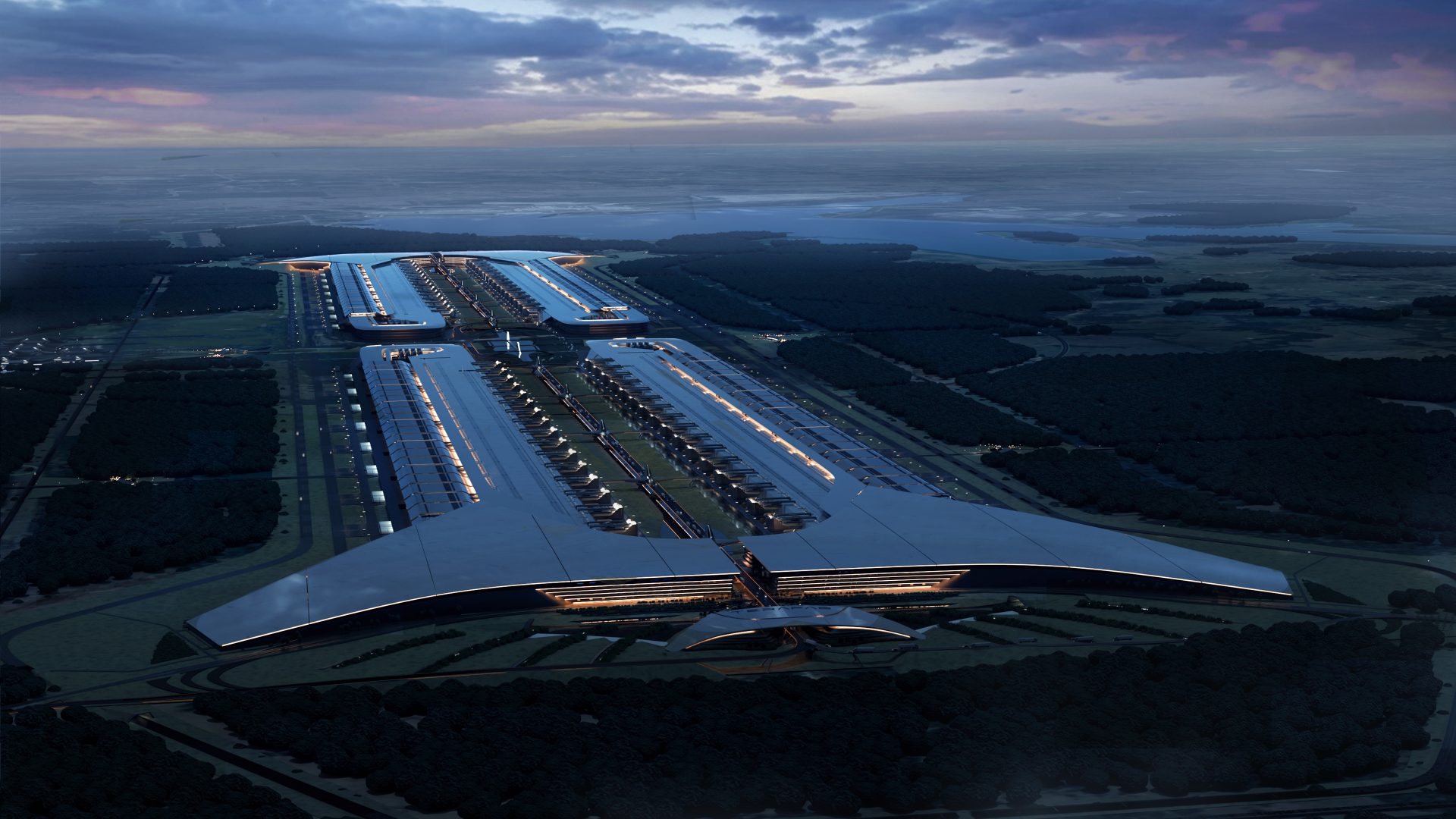
The project is currently at a nascent stage. An investment of $16.8 billion has been earmarked for a semiconductor complex in Grimes County, Texas. The complex would eventually expand to a footprint of 100 million square feet, which would make it one of the largest planned chip sites in the United States.
The venture is designed to bring the main steps of chip production under one roof. These include mask generation and lithography, advanced chiplet packaging, and testing. Chipmaking is usually split across specialized companies and sites, which adds time and coordination work to every design change. By keeping these processes together, Terafab aims to shorten the chip design loop from the current six to nine months to a matter of weeks.

Memory and logic split in the capacity plan
According to Nikkei, Terafab has told its suppliers that it is targeting 1 million wafers per month by 2032. That total would be divided into 700,000 wafers per month for memory chips and 300,000 wafers per month for logic chips. Memory chips such as DRAM store data for active processing, while logic chips handle calculations and control tasks.
For scale, Samsung’s total DRAM capacity is currently estimated at between 650,000 and 700,000 wafers per month. That means Terafab’s memory target alone would be roughly equal to the entire DRAM output of the South Korean chipmaker. Samsung is one of the largest memory producers globally and has spent decades building its manufacturing base.
Terafab is a new entrant in a market led by established producers. Reaching Samsung’s current scale within about six years would be a major achievement, and the plan depends on the companies building capacity on schedule.
Tensions with TSMC and the role of Intel
Musk has previously called TSMC a mere subcontractor, and Terafab is now reportedly renegotiating the terms of a possible partnership with the Taiwan-based contract chipmaker. The talks reportedly focus on the operational control hierarchy and the size of the investments required. These points remain unresolved.
Musk had earlier ruled out the possibility of TSMC holding a stake in Terafab or owning and running the facility. The reported renegotiations therefore show that the terms of any TSMC role are still being discussed, even though a stake has been ruled out.
On the logic side, Terafab also intends to use Intel’s 14A process for its logic chips. Intel’s 14A is one of the company’s advanced manufacturing processes, and its use would tie Terafab’s logic production to Intel’s foundry technology. Intel’s backing for the project is part of its broader effort to win outside customers for its chipmaking services.
What the plan means for chip buyers and the industry
For most consumers, Terafab’s plans are a long-term signal rather than a near-term product change. The chips would first be used internally by SpaceX and Tesla for robots and data center hardware. Any broader market impact would depend on whether the venture meets its timelines and whether it sells capacity to other customers.
For the memory market, a new producer of this size would matter if it reaches the scale described. Memory supply has historically moved in cycles, and new capacity can change pricing and availability. The 2032 target is still years away, and the plan has not yet been finalized with all partners, including TSMC.
The main open questions are the funding of the full $16.8 billion investment, the final terms with TSMC, and whether the schedule for a 1 million wafer monthly output holds. Terafab’s progress on these points will show whether the plan moves from supplier briefings to construction and production.